|
||||||||
IntroductionWhen Intel started talking about their higher end, workstation-bound Tumwater chipset, so too did NVIDIA start talking about "SLI". The term SLI will bring back memories for those that have been following the PC graphics industry long enough to have known that this is synonymous with 3dfx’s multi-graphics rendering systems – thanks to their purchase of 3dfx’s assets prior to 3dfx closing up shop, NVIDIA have pulled the acronym out of mothballs and, whilst giving it slightly different technology and terminology, applied it to basically the same thing: attaching multiple rendering devices together for higher rendering performances. In this article we’re going to take a look at NVIDIA’s SLI technology, and the performance gains afforded by it in the all the available GeForce 6 configurations. First, though, we’ll take a quick refresher of the scalable graphics implementations we’ve seen related to PC graphics so far. History of Multi-Visual Processor Rendering3dfx, Where it Began3dfx (back then, 3Dfx) were the first to introduce us to scaleable graphics on the PC and their name has long since been tied with "SLI". 3dfx's first graphics processor, Voodoo's SST1 chipset, was scalable in its very nature - with separate rendering and texture cores boards, from one to three texture units could be built and multiple boards could actually operate together. SST1 was being hawked around Arcade and Visualisation/Simulation vendors until, luckily for 3dfx, memory prices dropped suddenly making a board with a single rasteriser and texture unit a viable prospect as a separate PC graphics accelerator. Voodoo 2's SST96 chipset basically took the SST1 cores and placed them on a smaller process, thus making a single rasteriser and two texture unit boards affordable for the PC graphics market; however, buoyed by the success from Voodoo Graphics the idea of doubling the attach rate saw them resurrect the multi-board configurations that SST1 were capable of. Thus SLI was born.
Back then, SLI stood for "Scan-Line Interleave". Basically the principal involved two Voodoo 2 boards, each being plugged into PCI ports and being sent the full graphics dataset - each board would render separate, alternate scan lines, such that one board would render the odd lines displayed on the monitor, whilst the other would render the even. The process required the two boards to be plugged together via a small ribbon cable with the analogue image data being transferred from the slave board to the master, resulting in the odd and even lines interleaving at the display making up a single rendered image. However, as the process was used post the RAMDAC stage with analogue data, any slight timing issues could often be noticed as the odd and even lines could be slightly out of sync.
As the PC graphics industry moved on, so too did 3dfx have to and they concentrated on single 2D/3D accelerators for a while with Voodoo Banshee and Voodoo 3. It wasn't until their next chip, VSA-100, did "SLI" crop up again, although this time not as a multi-board solution but a single board with multiple chips. The SLI acronym, although getting the message across, wasn't entirely accurate as far as VSA-100 based products were concerned as it no longer relied purely on single Scan-Lines. Being based on a single board VSA-100's utilised a digital screen apportioning method that distributed horizontal bands, scalable between 1 and 256 pixels in height, between the graphics processors on a single board. VSA-100's scalable capabilities were also intrinsically linked to its "T-Buffer" operation that allowed for numerous effects, but most importantly Jittered SuperSampling FSAA - VSA-100's interaction between SLI and T-Buffer operations are explained in our T-Buffer Investigated article. VSA-100 could scale to 32 processors within a single rendering system, although for the PC only 1 (Voodoo4), 2 (Voodoo5 5500) and 4 chip (Voodoo5 6000) boards were planned, although the 4 chip implementation never made into retail availability due to power and AGP bridging issues. |
||||||||
| |
||||||||
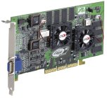
Beyond 3dfx3dfx were not the only PC graphics vendor to take a stab at multi graphics processor implementations over recent years. While ATI have been one of the longest sole remaining PC graphics provider, unlike recent years, they weren't always synonymous with the highest performance graphics so during a periods when they were getting squeezed by the emergent NVIDIA and others, ATI decided to take a stab at a multi-chip solution. ATI's solution, called Rage Fury MAXX, basically comprised of two Rage Fury chips placed on the same board; however, they fell foul of Windows 2000's handling of the AGP mastering and the solution would only operate with the Windows 9x kernel.
More recently the newcomer XGI attempted to stake a claim on the high end with their Volari V8 Duo, consisting of two 8 pipeline chips on a single board. Ultimately, though, the odds were stacked against them - this was their first modern hardware implementation, their fresh drivers had to cope with modern titles, and then throwing in the work for the dual chip rendering on top of that - which ultimately ended with disappointing performance. Both the Volari Duo implementations and ATI's Rage Fury MAXX used a rendering system called Alternate Frame Rendering (AFR) which we'll explain in a little more detail later. Dual Board ExperimentsWhilst 3dfx were busy with single chip AGP boards between Voodoo2 and VSA-100, with the Voodoo3 boards, a company called Metabyte tried to resurrect the multi board rendering idea. Due to issues with the AGP port only allowing one graphics interface per system (technically this restriction was removed with the latest AGP8X specification but evidently its cost of implementation was too high as nobody took up on it) the fastest available method for running two boards within a system was to utilise an AGP graphics board and a PCI board and Metabyte produced a solution that could get two Voodoo3’s or TNT2’s, one on each interface type, operating together to speed up the rendering time in comparison to a single board. However, as the boards it was designed to work with - boards that had no scalable capabilities - it required an extra board to composite the image from the two graphics accelerators back into a single, displayable image. Another issue is that as these chips had no tiling or "SLI" screen division capabilities, the rendering split was a straight split with one board rendering the top portion of the screen and the second rendering the bottom. It wasn’t a 50/50 split, though, and biased more to one board than the other in order to get over the uneven workloads that are naturally inherent in games (we’ll discuss this more later on). Ultimately, the system never made it to the market. The high end, gamers oriented system builder Alienware had taken the Metabyte system to heart and purchased the technology and it’s thought the inVento also followed to Alienware. Shortly after PCI Express systems were introduced, Alienware started touting their own dual board implementation: "Video Array", based on PCI Express, but following the similar principles as the initial Metabyte solution. Little did they know, though, that NVIDIA were ready to pull the rug from under their feet with their own solution! Beyond PCMulti-Chip solutions born from PC graphics have quite frequently made their way outside of the PC space as well, though. Fairly early in the life of 3dfx one of the founders went off to found Quantum3D, which primarily took 3dfx technology and pushed them into other usages such as embedded systems and high end Visualisation/Simulation systems. For instance, their AAlchemy system leverages up to 16 VSA-100 chips for high resolution, high depth FSAA rendering. Since the demise of 3dfx Quantum have been working closely with NVIDIA and they have been utilising NVIDIA graphics for their multi-chip rendering solutions, such as the newer Independence 2500 systems that can utilise multiple NV40 chips for rendering up to 64 sample FSAA.
PowerVR, an infrequent visitor to PC graphics rendering, have also had their hand in multi-graphics implementations with their Neon 250 architecture. SEGA adopted Neon 250 DC (the Dreamcast version of Neon 250, which was largely similar as the PC version) for their Naomi 2 arcade boards placing two Neon 250 raster chips in conjunction with an "Elan" T&L processor. PowerVR utilise a Tile Based Deferred Rendering scheme, and as they operate by breaking the rendering scene into tiled regions in the first place, this can also operate over the two chips on the Naomi 2 board, with each chip rendering alternate tiles. More recently ATI have also got into multi-chip rendering systems as their high end parts since R300 have been designed to scale to a maximum of 256 chips in a single rendering system. Although ATI operate an immediate mode rendering system, as most do, they also render by splitting the scene up into tiled regions that do not only span the quad pipelines within a single chip, but also multiple chips within a rendering system. SGI utilise up to 32 chips in their Onyx4 and up to 16 in the Prism visualisation systems, and Evans & Sutherland couple up to 64 together in their RenderBeast system. |
||||||||
| |
||||||||
NVIDIA's SLIAlthough NVIDIA are leveraging the popular SLI brand from 3dfx, they have slightly altered its meaning as rather than "Scan-Line Interleave" it now equates to "Scaleable Link Interface", but NVIDIA are harking back more towards the Voodoo2 style dual board implementation. Whilst AGP, even when it had the capability with its final implementation, never managed an implementation with more than one interface, PCI Express is inherently different and allows for much more flexibility in how it is supported. Where AGP is a single, wide, bi-directional, parallel bus implementation PCI Express utilises multiple point-to-point "lanes", each with dedicated upstream and downstream paths. Where AGP increased performance over its basic PCI configuration with increased clock speeds and multiple data transmits per cycle, the signalling of PCI Express for a graphics implementation is exactly the same as any other PCI Express expansion device, all that differs is the number of lanes that simultaneously go to the graphics device. Where we will see 1 lane (x1), 2 lanes (x2) or possibly 4 lanes (x4) for expansion devices such as Sound Cards, RAID controllers, Gigabit Ethernet devices, etc., the PCI Express standard calls for a dedicated 16 lanes (x16) to the graphics card, which results in both an upstream and downstream bandwidth of 4GB/s. Although the specification calls for the PCI Express chipset to support 16 lanes for graphics and the motherboards to support a x16 connector, due to the way the implementation is specified the graphics board doesn’t actually need to be connected to all 16 in order to operate - it could, theoretically, operate on just a single lane. This is what NVIDIA are using in order to take advantage of their first implementation of their new SLI. When NVIDIA initially talked about SLI in conjunction with the Intel Tumwater chipset it utilised the 20 PCI Express lanes in the chipset Northbridge by distributing x16 to a primary x16 graphics board connector and the final 4 from the North Bridge to a secondary x16 connector (obviously only connecting the first 4 lanes of the connector), leaving the full PCI Express for graphics bandwidth to the primary x16 connector and 1GB/s of upstream and downstream bandwidth for the secondary x16 connector. Late last year NVIDIA introduced their new AMD 64 platform processor, nForce4 and as they were supporting PCI Express with this core logic processor they took the opportunity to define a slightly different take on addressing two graphics connections.
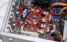
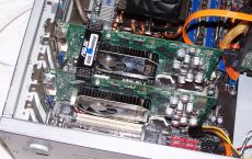
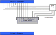
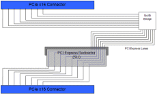
With the nForce4 SLI platform NVIDIA specified a particular routing mechanism to enable dual graphics board to operate on the platform. nForce4 SLI only dedicates a maximum of 16 lanes to any graphics solutions, and by default all of these are routed to the primary graphics connector (as displayed in Figure 1 above); however, the final 8 lanes are routed via a small PCI Express redirector card and when this is turned around this redistributes the final 8 lanes from the primary x16 slot to the first 8 lanes of the second x16 slot (Figure 2) such that two graphics boards can be placed in the system, each having 2GB/s of upstream and downstream bandwidth to the core logic via 8 PCI Express lanes each. NVIDIA also state that the nForce4 SLI core logic has some arbitration logic in order to better redirect the graphics data to both sets of PCI Express lanes, although how much of this is a hardware and how much is a software solution is unknown. Technically any motherboard board that distributes some lanes to multiple PCI Express x16 connectors, whether that includes an uneven distributions such as the Tumwater solution, an even distribution split such as nForce4, or even a multi-processor system with multiple core logic processors (thus having enough lanes to have two dedicated x16 graphics paths) could operate with NVIDIA’s graphics SLI system; however, at present NVIDIA state that it is only "validated" for the Intel Tumwater chipset and nForce4. Whilst the distribution of the PCI Express lanes for the graphics connectors on the motherboard takes care of the communication of both graphics boards to the host, there is one other element of communication involved with NVIDIA’s SLI. Whilst the two graphics boards in this SLI system are able to communicate with each other via the core logic, NVIDIA have also given them a direct connection, and this is where the "Scalable Link Interconnect" comes into play.
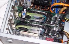
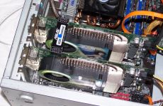
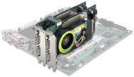
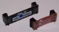
All of NVIDIA’s SLI enabled graphics boards have an extra set of exposed connections on the opposite side of the board to the PCI Express connector strip, and this is where the SLI connector goes. When the two graphics boards are in the system for SLI use they are connected by the SLI connector such that they have some direct communication capabilities with each other. Although NVIDIA haven’t actually stated the bandwidth of the interconnect, nor what it is actually used for, we do know that it is used for passing the digital frame buffer data from the "slave" (secondary) board to the "master" (primary board that is connected to the display) each frame - we can see that as removing the connector during operation will cause the elements that the slave board is rendering not to be displayed, whilst the elements that the primary board is rendering continue to be displayed. (Evidently NVIDIA states that on an Intel system the "Master" board is always chosen as that closest to the CPU, yet on an AMD the Master and Slave selection is done at boot time). The connectors themselves are currently only shipping with nForce4 SLI motherboards, and because vendors may choose to locate the two graphics connectors in different slot positions the connectors may vary in length. Whilst some connectors have a rigid PCB, which may not be ideal if the case and motherboard fit isn’t ideal, there are also flexible strip varieties available, though so far we have only seen these ones from NVIDIA themselves, for testing purposes.
Each of the graphics cores that feature SLI have an area of die dedicated to the communication and control in order for SLI to operate. |
|||||||||||||||
| |
|||||||||||||||

| |
||||||||||
NVIDIA SLI Rendering ModesWhen SLI was initially announced NVIDIA primarily talked about a split screen rendering mode, distributing some of the top portion of the screen to the one board and the rest to the second, load balancing the split on a per frame basis; however, it soon transpired that they were also using an Alternate Frame Rendering mode in some cases. Let's take a slightly closer look at the two modes. SFR - Split Frame Rendering
The first rendering mode that NVIDIA's SLI implementation utilises is that of "Split Frame Rendering" (SFR). As the name suggests this splits the rendering of the frame between the two boards, much like 3dfx's SLI solutions did. However, unlike 3dfx's solutions, the initial GeForce 6 implementation appears not to have any capabilities to divide the screen multiple times, so there is a much more straight split with one board rendering the top portion of the image and the second rendering the remainder. When each of the boards has finished rendering its portion of the frame the "slave" board passes its rendered data, digitally, over the SLI connector to the master which then composites this with the portion of the frame it has rendered and then these are sent to the RAMDAC or TMDS for display. One issue that scalable graphics implementations that rely on rendering via splitting the screen across multiple graphics processors have to overcome is that of uneven workload distribution across the screen. If we consider a classic First Person Shooter game then what we can often find is that the lower portion of the screen, usually where much of the other characters are found or where the complex environment geometry is seen, has a high overdraw complexity, whereas the upper portion, which often has less complex world geometry or even just a sky-box, and will not be populated by other characters for much of the game, has a low overdraw complexity. Overdraw occurs when there are multiple objects in front of one another as graphics cards invariably spend time checking or calculating the pixels that will be ultimately only be overwritten by other pixels – i.e. if we have a case where a wall is rendered first then a character is rendered in front of it afterwards, we have an geometry overdraw complexity of two and the pixels for both the wall and character nominally need to be generated, even though the character will obscure some of the pixels calculated for the character; place another character in front of our previous one and we have a geometry overdraw complexity of 3x, with more pixels that may need to be calculated and rejected. Modern graphics processors have large chunks of silicon dedicated to minimising the effects of overdraw as much as possible by rejecting pixels that are already deemed to be obscured by pixels previously calculated with early Z rejection schemes (at the pixel level, or in groups prior to the fragment pipeline); however, these are only maximised when the developer sorts the geometry in a front to back fashion, and even then cycles have to be spent doing early rejections (although much, much fewer than leaving them to calculate).
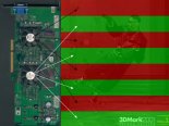
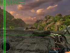
Even at the visible pixel level workload distributions can vary significantly for different portions of the screen. For instance, it is conceivable that sky-boxes on some occasions may only require a few cycles to generate the final colour value, but a pixel shaded area of water, reflecting the world around it, can take many more cycles. Figure 3 shows a scene from Half Life 2 which highlights such uneven workload distribution with, at the bottom half of the screen, a fairly complex water shader with reflections from the rest of the scene and a shader generated spray from the helicopter, whilst the top portion of the screen is relatively empty. Due to these types of issues, without load balancing there would be many occasions where one graphics chip may finish the portion of the screen it is rendering much earlier than the other(s) in the rendering subsystem, resulting in it being idle whilst the rest of the frame is rendered, which doesn’t maximise the rendering potential of all the graphics processors available. Scan line, banded and tiled systems can be implicitly load balanced as the distribution of the frame strips or tiles across each of the graphics chips in the system means that any differences in rendering load across the screen are already fairly well balanced anyway, minimising the time one processor finishes before the rest of the rendering is completed. A simple implementation that just splits the rendering across two processors with one rendering an upper portion of the screen and the other rendering the rest is likely to suffer the worst with uneven workloads, and a straight 50/50 distribution is not likely to be the best solution – indeed the Metabyte solution mentioned earlier hard coded an uneven split between the two graphics boards in the system. NVIDIA’s Split Frame Rendering (SFR) mode addresses this issue by altering the number of lines each of the two boards rendering on a per frame basis. It's likely that the load balancing split calculation is based on timings from the previous frame: i.e., should the first frame rendered start with a 50/50 split the difference in time it took for each board to render its half of the screen will be used to calculate the percentage split for the next frame; if the slave board took longer to render its portion image from the first frame it will be asked to render less of the image, with the master calculating more, in the next frame proportionally adjusted by how long it took to render the first.
With SLI systems NVIDIA have provided a feedback option that displays the level of load balancing between the two boards. In SFR mode this is represented by a horizontal line that moved up or down the screen to illustrate how much of the image each board is actually rendering. With the SFR mode of SLI, rendering pixel fill-rate and Pixel Shader fill-rate is doubled. However as it is not known where vertex data will end up on the screen prior to processing by the Vertex Shader both boards in the SLI system will need to do all the Vertex Shader / T&L processing for the entire scene, so this does not scale in this mode. By the time vertex data reaches the clipping stage it is known where it will appear onscreen, so vertex data that will not appear on the portion of the screen being rendered on each graphics board can be discarded by that board, so if the application is vertex limited post the clipping stage then some gains can be made; however, if it's limited at the Vertex Shader / T&L stage then there won’t be gains to be made here. |
||||||||||
| |
||||||||||

|
|||||||||
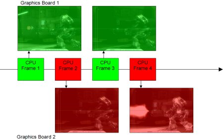
AFR - Alternate Frame RenderingAlternate Frame Rendering (AFR) is fairly explanatory in its name in that both boards will render an entire frame of data, but do so by alternating between the two boards. Most graphics boards, like as the GeForce 6 series, process as "immediate mode renderers" such that, although there is plenty of data buffering going on, as information is supplied from the CPU to the graphics cards, the graphics card will begin that rendering, hence the CPU and graphics will usually be working on the same frame, more or less. AFR operates by having the board that is rendering the to-be-displayed image operating one frame behind the one the CPU and the CPU sends the data to alternate boards. Under AFR processing the rendering process goes along the following lines:
Once the CPU begins processing the initial frame it will send its data to the master graphics board to begin rendering and whilst the master board is rendering the CPU will begin the next frame and begin transmitting that to the slave board. Whilst the slave board is rendering the second frame, and if the CPU has also finished processing for that frame, assuming the master board has finished rendering the first frame, the CPU can begin processing the third frame and sending the data pertinent to that frame to the master board. The master board is still responsible for the display of the final rendered image, so upon completion of its frame the slave board will transmit its frame buffer data across the SLI connector to the master board and then the master board will ready that for display. With AFR rendering, if the processing is CPU limited then there will be no gains or losses (bar the slight processing overhead of switching the frame data from one board to the other) as in effect the processing will still be as it would be in single board immediate mode rendering. If the processing is graphics limited, though, there will be one frame of latency as the image being rendered and displayed is not the image being processed, though you should be gaining more overall frames per second anyway.
The driver feedback representation for AFR mode is displayed with the horizontal line staying static in the middle over the screen, but the vertical bar moving in from the top and bottom. It's not quite as obvious to decipher the exact meaning of this but we suspect the vertical bar position represents how graphics or CPU limited the frame is, hence how much benefit AFR SLI is giving in that title and mode of rendering. In the case of AFR, as each board is rendering an entire frame both vertex rate and pixel rates are theoretically doubled, assuming the rendering system is sufficiently bottlenecked such that there is enough CPU capacity to provide sufficient data to each graphics board. |
|||||||||
|
|||||||||
|
|||||||||||||||||||||||||||||||||||||||||||||||||||||||||||||||||||||
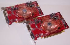
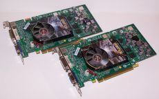
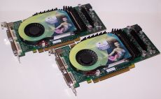
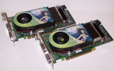
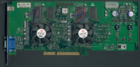
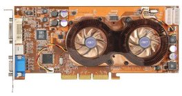
SLI HardwareThe Graphics BoardsIn order for SLI to operate you'll first need two graphics cards that can work together in SLI mode. At present, and it is likely to remain this way, it is currently the higher end of the mainstream and enthusiast boards that have SLI capabilities, which in total results in four different board configurations. The following are the NVIDIA SLI enabled boards and their top line specifications:
* Note that for the GeForce 6 6600 GT and 6800 we are using partner boards which don't quite meet the reference specifications. In the case of the 6600 GT it is actually clocked up slightly with a core speed of 515MHz, as opposed to the reference specification of 500MHz, while the 6800 has core and memory clocks of 334/309MHz as opposed to the default of 325/350MHz. Although the reference specification for GeForce 6800 Ultra the reference boards used in this article automatically clocked themselves to 437/565MHz on the SLI platform. As NVIDIA's SLI operates by making use of the flexibility of PCI Express the only boards that presently feature SLI are the PCI Express versions of the GeForce 6 series, starting from the 6600 GT and above.
For those considering SLI as a gradual upgrade process you much bear in mind that the boards have to be the same as one another, so the second board purchased has to be from the same manufacturer as the original board (i.e. ASUS and ASUS, or MSI and MSI) and the same model version (i.e. ASUS Extreme N6600 GT and ASUS Extreme N6600 GT, or MSI NX6600GT TD128E and MSI NX6600GT TD128E). |
|||||||||||||||||||||||||||||||||||||||||||||||||||||||||||||||||||||